Spectroscopy and Test Devices

Semiconductor Test Devices

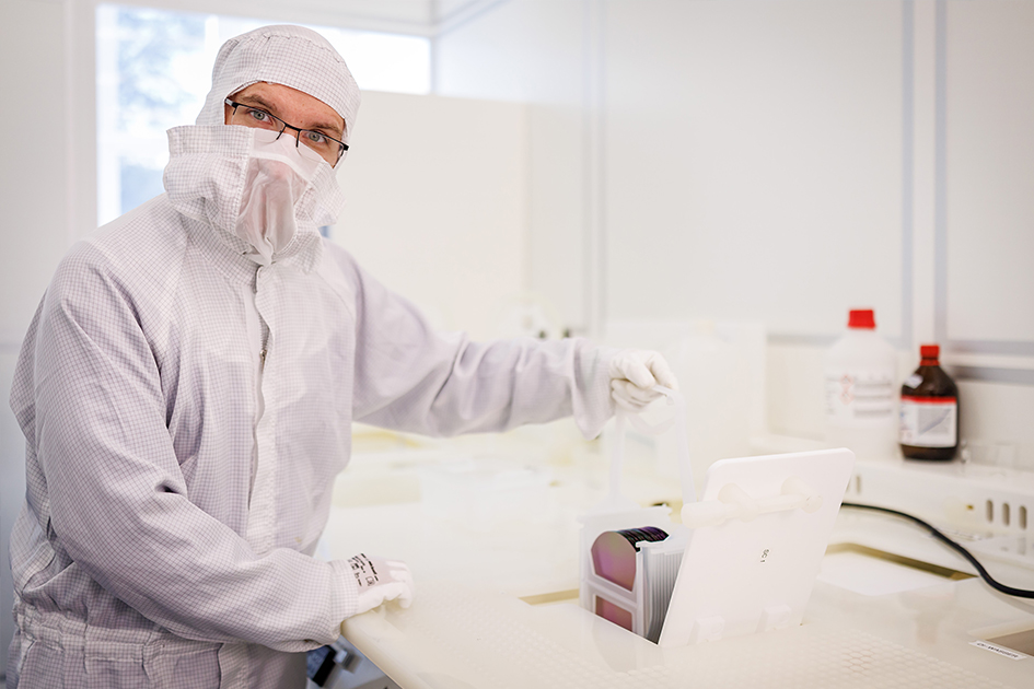
We carry out our activities for structuring and processing customer-specific test devices in the central clean room laboratory at the TU Bergakademie Freiberg.

Based on a comprehensive defect-spectroscopic characterization of semiconductor materials (notably GaN, SiC, AlGaN, AlN, GaAs, and InP), test devices can be produced and characterized at an early stage of material development in partnership with the Institute of Applied Physics at TU Bergakademie Freiberg. This facilitates a systematic correlation between material properties and the resulting device characteristics, as well as the identification of defects critical to the devices.

Additionally, the IISB branch in Freiberg allows for addressing custom queries related to process development and the design of test devices. In our flexible, fully CMOS-integrated cleanroom facility, we can both individually adapt processes and correlate material properties with device performance to identify critical material defects.

Key topics and competences

  • Wide-Bandgap (WBG) / Ultrawide-Bandgap (UWBG) based (test)devices
  • Atomic layer processing: Atomic Layer Deposition (ALD) and Atomic Layer Etching (ALE)
  • Device characterization using current-voltage and capacitance-voltage curves (IV/CV), as well as interface defects (Dit) and deep-level defects in the bandgap using Deep Level Transient Spectroscopy (DLTS) and related methods

Services

  • Customer-specific challenges in process development
  • Development of device processing steps (ALD, ALE, passivation, etching, metallization)
  • Single process evaluation using various test devices
  • Support for single process technology development
  • Customized design of test devices
  • Identification of device-critical defects and their correlation to device properties and device characterization
  • Electrical characterization of devices at wafer level by IV, CV measurements and determination of interface traps
© Daniel Karmann / Fraunhofer IISB
Central clean room laboratory at TUBAF in Freiberg
© Daniel Karmann / Fraunhofer IISB
Chemical cleaning of the wafers
© Daniel Karmann / Fraunhofer IISB
Transferring of the structure mask at the laser lithography
© Daniel Karmann / Fraunhofer IISB
Structuring on the ALD/CVD deposition or ALE etching cluster
© Daniel Karmann / Fraunhofer IISB
Characterization using a spectral laser ellipsometer
© Daniel Karmann / Fraunhofer IISB
Metallization via thermal or electron beam evaporation
© Daniel Karmann / Fraunhofer IISB
Separation of devices through dicing
© Daniel Karmann / Fraunhofer IISB
Separation of devices through dicing
© Daniel Karmann / Fraunhofer IISB
Labeling of wafers using a laser writer

Electrical characterization and spectroscopy

We offer the electrical characterization of devices at wafer level by IV, CV measurements, the determination of interface traps and in-depth electrical defect spectroscopy for small samples to determine the defect level.

The variability of semiconductor substrates for applications in power and communication electronics has been rapidly increasing in recent years. In this context, compound semiconductors play a significant role. These materials exhibit physical properties that surpass those of established silicon for these applications. Moreover, defects in these materials are candidates for the realization of individual quantum states for future highly sensitive quantum sensors or ultra-high-performance quantum computers.

We provide extensive expertise in characterizing the electrical properties of various crystal and wafer materials, as well as partially and fully processed devices. This enables us to perform service measurements with a short turnaround time for our clients. Additionally, we leverage this toolkit, particularly the capability to fabricate various test devices, to identify critical defects affecting the performance and reliability of the components, understand their origins, and collaborate with our clients to find solutions to mitigate these critical defects.

Key topics and competences

  • Semiconductor material characterization, especially electrical defect spectroscopy of crystals and epitaxial layers using:
    • DLTS, optical DLTS
    • IV and CV measurements
© Daniel Karmann / Fraunhofer IISB
Device contacting with bonding wire
© Daniel Karmann / Fraunhofer IISB
Automated wafer prober
© Daniel Karmann / Fraunhofer IISB
GaN HEMT and test devices on sapphire substrate

Publications

Flyers & Brochures

OSZAR »